DESCRIPTION
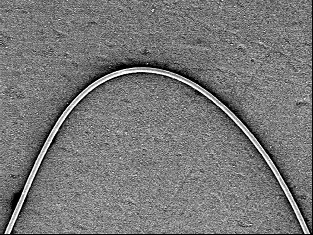
This is a scanning electron microscope image of a silica nanowire on a silica aerogel surface. New technologies have made it possible to draw glass in long, ultra-smooth wires with uniform diameters in the nanometer range. Because of their extraordinary uniformity, these nanowires have unique properties important in optics and photonics, both of which require precise control of light. • SIZE: The nanowire is 530 nm long and the radius of the bent wire is 8 µm. • IMAGING TOOL: Scanning Electron Microscope
OBJECTIVES
NANO CONTENT MAP
Nanometer-sized things are very small, and often behave differently than larger things do.
Nanoscience, nanotechnology, and nanoengineering lead to new knowledge and innovations that weren't possible before.
DOWNLOAD FILES
Credits
Eric Mazur, Harvard University - Attribution is required. The creator listed here has made this image available to NISE Network partners for non-profit educational use only. Uses may include but are not limited to reproduction and distribution of copies, creation of derivative works, and combination with other assets to create exhibitions, programs, publications, research, and websites.
The creator listed above has made this image available to NISE Network partners for non-profit educational use only. Uses may include but are not limited to reproduction and distribution of copies, creation of derivative works, and combination with other assets to create exhibitions, programs, publications, research, and websites.

