DESCRIPTION
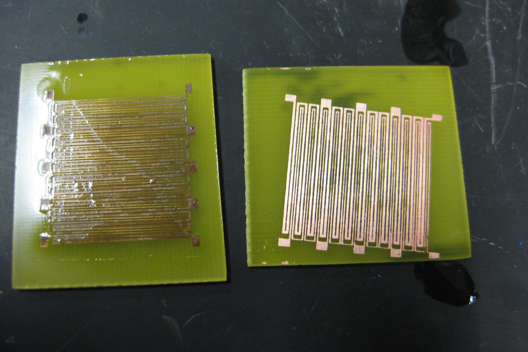
This activity is designed for high school students. In this experiment students use UV light to transfer a pattern (either a network of very small metal wires or self-drawn patterns) onto a surface-- a plastic board. The pattern is transferred by placing a mask (transparency sheet with the pattern) on a plastic board. The board is coated with a copper film that is covered with a light-reactive polymer (photo-resist). The polymer is exposed to UV light through the mask to make a pattern in the polymer. The metal under the exposed polymer is then chemically etched, leaving only the pattern on the surface of the board as determined by the mask. This top-down approach to nanotechnology is commonly used in manufacturing circuit boards for computers and other electronics.
DESCRIPTION
This activity is designed for high school students. In this experiment students use UV light to transfer a pattern (either a network of very small metal wires or self-drawn patterns) onto a surface-- a plastic board. The pattern is transferred by placing a mask (transparency sheet with the pattern) on a plastic board. The board is coated with a copper film that is covered with a light-reactive polymer (photo-resist). The polymer is exposed to UV light through the mask to make a pattern in the polymer. The metal under the exposed polymer is then chemically etched, leaving only the pattern on the surface of the board as determined by the mask. This top-down approach to nanotechnology is commonly used in manufacturing circuit boards for computers and other electronics.
OBJECTIVES
BIG IDEA
Demonstrate the top-down approach to fabrication of nanometer sized electronic components commonly used in manufacturing circuit boards for computers and other electronics and teach the basic chemistry and physics necessary for photolithography.
LEARNING GOALS
Understand what lithography is and become familiar with different types of lithography.
NANO CONTENT MAP
Nanometer-sized things are very small, and often behave differently than larger things do.
Nanoscience, nanotechnology, and nanoengineering lead to new knowledge and innovations that weren't possible before.
DOWNLOAD FILES
Credits
Lawrence Hall of Science
Developed for the NISE Network with funding from the National Science Foundation under Award Numbers 0532536 and 0940143. Any opinions, findings, and conclusions or recommendations expressed in this product are those of the authors and do not necessarily reflect the views of the Foundation.
Creative Commons Attribution Non-Commercial Share Alike 3.0 United States (CC BY-NC-SA 3.0 US).
View more details
![]()
NISE Network products are developed through an iterative collaborative process that includes scientific review, peer review, and visitor evaluation in accordance with an inclusive audiences approach. Products are designed to be easily edited and adapted for different audiences under a Creative Commons Attribution Non-Commercial Share Alike license. To learn more, visit our Development Process page.